- 您现在的位置:买卖IC网 > Sheet目录3880 > PIC24F08KL302-I/SO (Microchip Technology)IC MCU 16BIT 8KB FLASH 28-SOIC
CHAPTER 6 CLOCK GENERATION FUNCTION
User’s Manual U15905EJ2V1UD
205
6.3
Control Registers
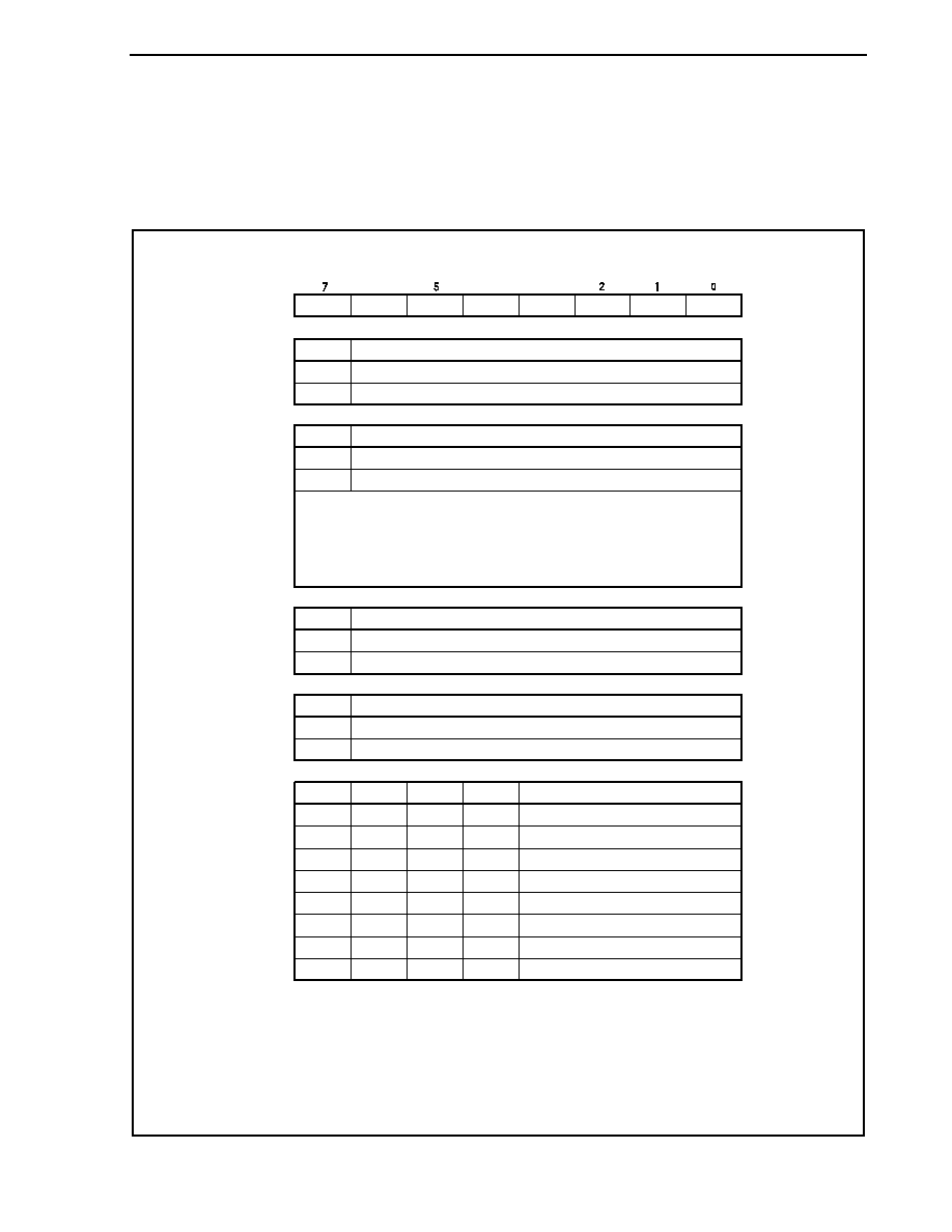
(1) Processor clock control register (PCC)
The processor clock control register (PCC) is a special register. Data can be written to it only in combination of
specific sequences (refer to 3.4.8 Special registers).
This register can be read or written in 8-bit or 1-bit units. The CLS bit is a read-only bit.
FRC
Used
Not used
FRC
0
1
Selects internal feedback resistor of subclock
PCC
MCK
MFRC
CLSNote
CK3
CK2
CK1
CK0
Operating
Stopped
MCK
0
1
Operation of main clock
Used
Not used
MFRC
0
1
Selects internal feedback resistor of main clock
After reset: 03H
R/W
Address: FFFFF828H
Main clock operation
Subclock operation
CLS
0
1
Status of CPU clock (fCPU)
fXX
fXX/2
fXX/4
fXX/8
fXX/16
fXX/32
Setting prohibited
fXT (subclock: 32.768 kHz)
CK2
0
1
X
Selects clock (fCLK/fCPU)
CK1
0
1
0
1
X
CK0
0
1
0
1
0
1
X
CK3
0
1
Even if the MCK bit is set to 1 while the system is operating with the main clock as
the CPU clock, the operation of the main system clock does not stop. It stops after
the CPU clock has been changed to the subclock.
When the main clock is stopped and the device is operating on the subclock, clear
the MCK bit to 0 and wait until the oscillation stabilization time has been secured
by the program before switching back to the main clock.
<6>
<4>
<3>
Note
The CLS bit is a read-only bit.
Caution
Do not change the CPU clock (by using the CK2 to CK0 bits of the PCC register) while
CLKOUT is being output.
Remark
X: Don’t care.
发布紧急采购,3分钟左右您将得到回复。
相关PDF资料
XF2L-0535-1
CONN FPC 5POS 0.5MM SMT
PIC18LF23K22-I/SS
IC PIC MCU 8KB FLASH 28SSOP
PIC16LF1933-I/ML
IC PIC MCU FLASH 4K 28-QFN
PIC16F1933-I/ML
IC MCU 8BIT FLASH 28-QFN
PIC16F785-I/ML
IC PIC MCU FLASH 2KX14 20QFN
XF2L-0425-1
CONN FPC 4POS 0.5MM SMT
PIC16F1933-I/MV
IC MCU 8BIT FLASH 28-UQFN
PIC16F785-I/SO
IC PIC MCU FLASH 2KX14 20SOIC
相关代理商/技术参数
PIC24F08KL302-I/SP
功能描述:16位微控制器 - MCU 8KB FLASH 1KB RAM 256B 3V RoHS:否 制造商:Texas Instruments 核心:RISC 处理器系列:MSP430FR572x 数据总线宽度:16 bit 最大时钟频率:24 MHz 程序存储器大小:8 KB 数据 RAM 大小:1 KB 片上 ADC:Yes 工作电源电压:2 V to 3.6 V 工作温度范围:- 40 C to + 85 C 封装 / 箱体:VQFN-40 安装风格:SMD/SMT
PIC24F08KL302-I/SS
功能描述:16位微控制器 - MCU 8KB FLASH 1KB RAM 512B 3V 10-BIT ADC RoHS:否 制造商:Texas Instruments 核心:RISC 处理器系列:MSP430FR572x 数据总线宽度:16 bit 最大时钟频率:24 MHz 程序存储器大小:8 KB 数据 RAM 大小:1 KB 片上 ADC:Yes 工作电源电压:2 V to 3.6 V 工作温度范围:- 40 C to + 85 C 封装 / 箱体:VQFN-40 安装风格:SMD/SMT
PIC24F08KL302T-I/ML
功能描述:16位微控制器 - MCU 8KB FLASH 1KB RAM 512B 3V 10-BIT ADC RoHS:否 制造商:Texas Instruments 核心:RISC 处理器系列:MSP430FR572x 数据总线宽度:16 bit 最大时钟频率:24 MHz 程序存储器大小:8 KB 数据 RAM 大小:1 KB 片上 ADC:Yes 工作电源电压:2 V to 3.6 V 工作温度范围:- 40 C to + 85 C 封装 / 箱体:VQFN-40 安装风格:SMD/SMT
PIC24F08KL302T-I/MQ
功能描述:16位微控制器 - MCU 8KB FL 1KB RAM 256B 3V RoHS:否 制造商:Texas Instruments 核心:RISC 处理器系列:MSP430FR572x 数据总线宽度:16 bit 最大时钟频率:24 MHz 程序存储器大小:8 KB 数据 RAM 大小:1 KB 片上 ADC:Yes 工作电源电压:2 V to 3.6 V 工作温度范围:- 40 C to + 85 C 封装 / 箱体:VQFN-40 安装风格:SMD/SMT
PIC24F08KL302T-I/SO
功能描述:16位微控制器 - MCU 8KB FLASH 1KB RAM 512B 3V 10-BIT ADC RoHS:否 制造商:Texas Instruments 核心:RISC 处理器系列:MSP430FR572x 数据总线宽度:16 bit 最大时钟频率:24 MHz 程序存储器大小:8 KB 数据 RAM 大小:1 KB 片上 ADC:Yes 工作电源电压:2 V to 3.6 V 工作温度范围:- 40 C to + 85 C 封装 / 箱体:VQFN-40 安装风格:SMD/SMT
PIC24F08KL302T-I/SS
功能描述:16位微控制器 - MCU 8KB FLASH 1KB RAM 512B 3V 10-BIT ADC RoHS:否 制造商:Texas Instruments 核心:RISC 处理器系列:MSP430FR572x 数据总线宽度:16 bit 最大时钟频率:24 MHz 程序存储器大小:8 KB 数据 RAM 大小:1 KB 片上 ADC:Yes 工作电源电压:2 V to 3.6 V 工作温度范围:- 40 C to + 85 C 封装 / 箱体:VQFN-40 安装风格:SMD/SMT
PIC24F08KL401
制造商:MICROCHIP 制造商全称:Microchip Technology 功能描述:Low-Power, Low-Cost, General Purpose 16-Bit Flash Microcontrollers with nanoWatt XLP Technology
PIC24F08KL401-I/MQ
功能描述:16位微控制器 - MCU 8KB FLASH 1KB RAM 512B 3V 10-BIT ADC RoHS:否 制造商:Texas Instruments 核心:RISC 处理器系列:MSP430FR572x 数据总线宽度:16 bit 最大时钟频率:24 MHz 程序存储器大小:8 KB 数据 RAM 大小:1 KB 片上 ADC:Yes 工作电源电压:2 V to 3.6 V 工作温度范围:- 40 C to + 85 C 封装 / 箱体:VQFN-40 安装风格:SMD/SMT